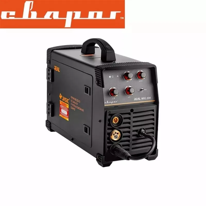
Сварочный аппарат Шеду МИГ-200 on.
23477

Новое поступление

Магазина LooKing somthing Store работает с 16.07.2019. его рейтинг составлет 88.92 баллов из 100. В избранное добавили 645 покупателя. Средний рейтинг торваров продавца 4.6 в продаже представленно 2563 наименований товаров, успешно доставлено 1191 заказов. 334 покупателей оставили отзывы о продавце.
Характеристики
*Текущая стоимость 8883.76 уже могла изменится. Что бы узнать актуальную цену и проверить наличие товара, нажмите "Добавить в корзину"
| Месяц | Минимальная цена | Макс. стоимость | Цена |
|---|---|---|---|
| Aug-17-2025 | 11281.7 руб. | 11507.27 руб. | 11394 руб. |
| Jul-17-2025 | 9149.42 руб. | 9332.47 руб. | 9240.5 руб. |
| Jun-17-2025 | 11104.21 руб. | 11326.77 руб. | 11215 руб. |
| May-17-2025 | 11015.81 руб. | 11235.58 руб. | 11125 руб. |
| Apr-17-2025 | 8794.25 руб. | 8970.46 руб. | 8882 руб. |
| Mar-17-2025 | 10837.87 руб. | 11054.59 руб. | 10945.5 руб. |
| Feb-17-2025 | 10748.78 руб. | 10963.52 руб. | 10855.5 руб. |
| Jan-17-2025 | 10660.32 руб. | 10873.46 руб. | 10766.5 руб. |
Описание товара

Brand NameNoneMeasurement unitpiece/piecesEach pack19 450,88 ₽-6%9 450,88 ₽-6%8 883,76 ₽8 883,76 ₽loader
The product specifications: diameter 2" × 0.4mm, crystal direction: <0001>, that is, c-axis, accept size customization.
This product is a GaN epitaxial wafer grown on sapphire (Al2O3) single crystal. It is used for making LED chips and conducting scientific experiments using MOCVD technology.
We offer high performance sapphire substrates and epitaxial wafers, and can be processed to different sizes and shapes according to your requirements to ensure excellent performance: strong adhesion, less defects, uniform and compact.
Basic parameters of GaN:
Ra is on the order of 0.5 nanometers;
Thickness: 3-5um; the company can provide four kinds of gallium nitride components: N type (doped with Si), P type (doped with Mg), I (undoped), Q (quantum well structure);
Dislocation density: 10th order of magnitude / cm2;
Carrier concentration: 10 to the power of 17 to 18 times / cc;
Resistance: 0.005 ohm.cm-1.
The basic situation of the sapphire substrate used is as follows:
Material High Purity Single Crystal Al2O3
Orientation C face (0001) ± 0.3 °
Offset angle to the M axis 0.20 ± 0.05°
Deviation from the A axis 0.0 ± 0.1°
Dismeter 50.8±0.15mm
Thickness 430μm±15μm
Total thickness deviation TTV <10μm
Surface total flatness TIR ≦10μm
WARP ≦15μm
BOW -10 ~ 0μm
Primary Flat Location A side (11-20)
Flat Off-set Angle 0.0 ± 0.2°
Primary Flat Length 16±0.5mm
Frontside Surface Roughness RA≦3 (ie Ra≦0.3nm)
Backside Surface Roughness (Ra) Ra=0.5~1.0μm
'
modname=images&cols=1&colspace=10&rowspace=10&align=centerСмотрите так же другие товары: