Tungsten disulfide 09: mica substrate WS2 | Обустройство дома


Сохраните в закладки:

Цена:US $522.72RUB
*Стоимость могла изменится

Количество:


Новое поступление

Advanced 2D Materials CO.,Ltd Store

Advanced 2D Materials CO.,Ltd Store

Магазина Advanced 2D Materials CO.,Ltd Store работает с 04.12.2018. его рейтинг составлет 100 баллов из 100. В избранное добавили 353 покупателя. Средний рейтинг торваров продавца 4.8 в продаже представленно 1617 наименований товаров, успешно доставлено 52 заказов. 4 покупателей оставили отзывы о продавце.

Характеристики

Tungsten disulfide 09: mica substrate WS2 | Обустройство дома

История изменения цены

*Текущая стоимость US $522.72 уже могла изменится. Что бы узнать актуальную цену и проверить наличие товара, нажмите "Добавить в корзину"

Месяц Минимальная цена Макс. стоимость Цена
Sep-16-2025 621.31 руб. 652.73 руб. 636.5 руб.
Aug-16-2025 616.70 руб. 647.77 руб. 631.5 руб.
Jul-16-2025 517.79 руб. 543.23 руб. 530 руб.
Jun-16-2025 606.37 руб. 636.79 руб. 621 руб.
May-16-2025 527.49 руб. 553.13 руб. 540 руб.
Apr-16-2025 595.62 руб. 625.41 руб. 610 руб.
Mar-16-2025 590.64 руб. 620.10 руб. 605 руб.
Feb-16-2025 585.25 руб. 614.48 руб. 599.5 руб.
Jan-16-2025 579.23 руб. 608.45 руб. 593.5 руб.

Описание товара

Tungsten disulfide 09: mica substrate WS2 | Обустройство домаTungsten disulfide 09: mica substrate WS2 | Обустройство домаTungsten disulfide 09: mica substrate WS2 | Обустройство домаTungsten disulfide 09: mica substrate WS2 | Обустройство дома


Production method:

Chemical Vapor Deposition (CVD)   Product introduction: Six carbon technology WS2 film is divided into a variety of: 1) A single layer of discretely distributed triangular single crystal grains having a triangular side length of typically several tens to one hundred micrometers. 2) A single-layer continuous film that continues to grow in Dalian by triangular grains. 3) Multilayer WS2 continuous film. 4) Substrate: WS2 has more optional substrates, and the sapphire substrate is a direct deposition product. Other substrates such as SiO2/Si, silicon wafers, PET, PI, ITO, FTO, glass, metal substrates, etc. are transferred to the substrate required by the customer after growth on sapphire.   Application areas: Optoelectronic devices, microelectronic devices, biosensing, chemical sensing and other fields.   Packaging and specifications 10*10mm, 15*15mm, 20*20mm, 2-inch wafer, 4-inch wafer or customer-specified custom size. Purification vacuum packaging, 1 piece / box, 5 pieces / box. 10 pieces / box.   Typical customers include: MIT, Caltech, Stanford University; Oxford University, Manchester University; Seoul National University, Korea Institute of Science and Technology (KAIST), and Sungkyunkwan University; Tokyo Institute of Technology, Murata Manufacturing Co., Ltd. Tsinghua University, Peking University, Institute of Semiconductors, Chinese Academy of Sciences And other world-class research institutions.

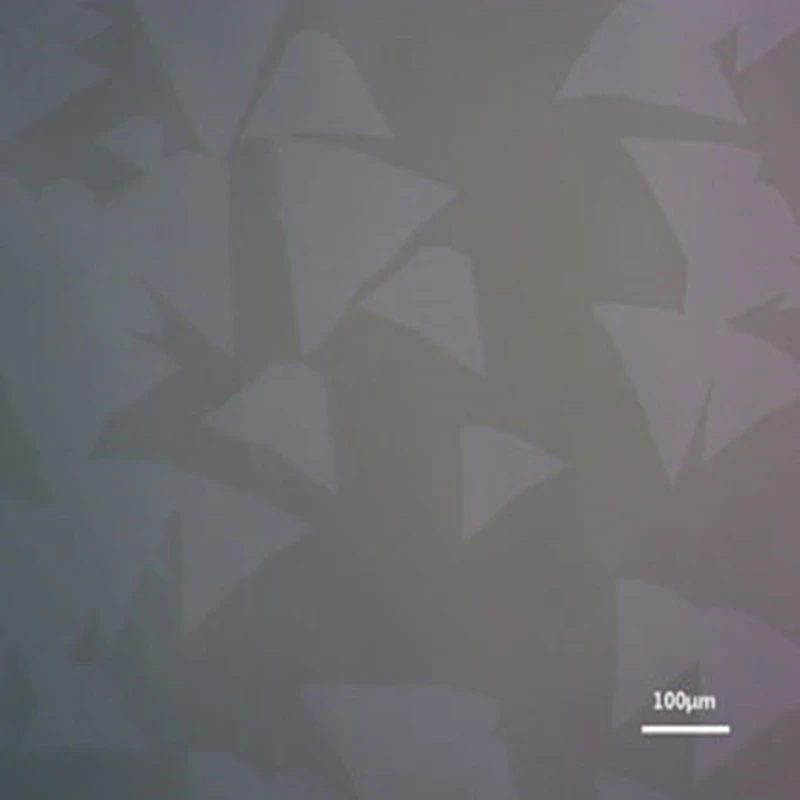
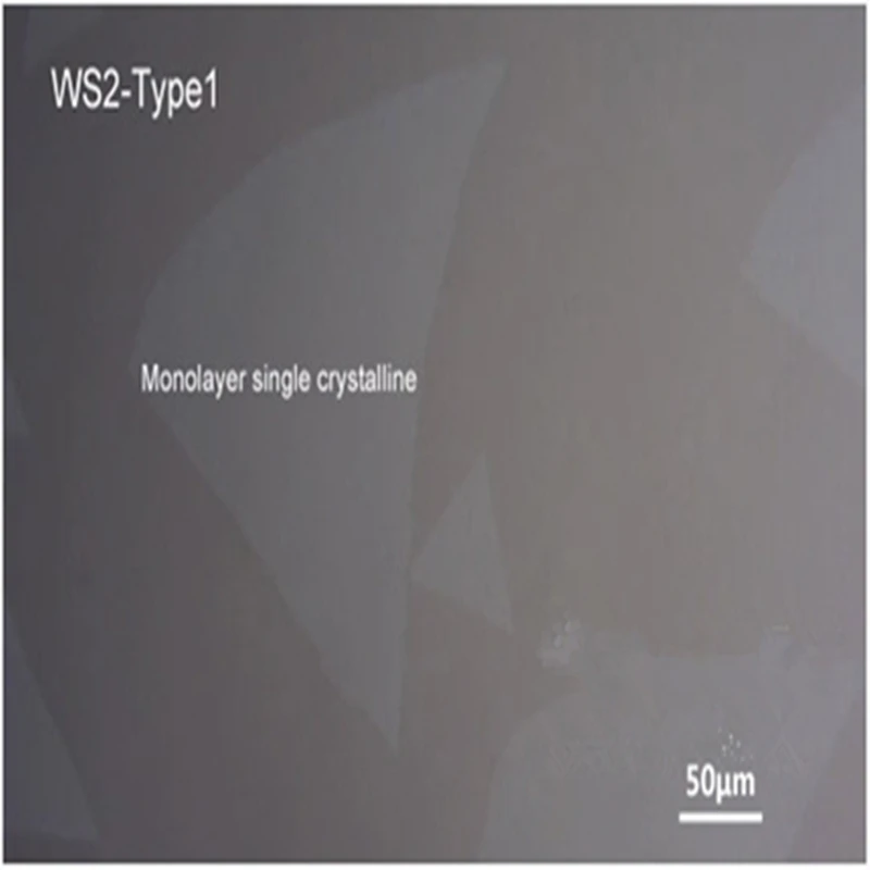
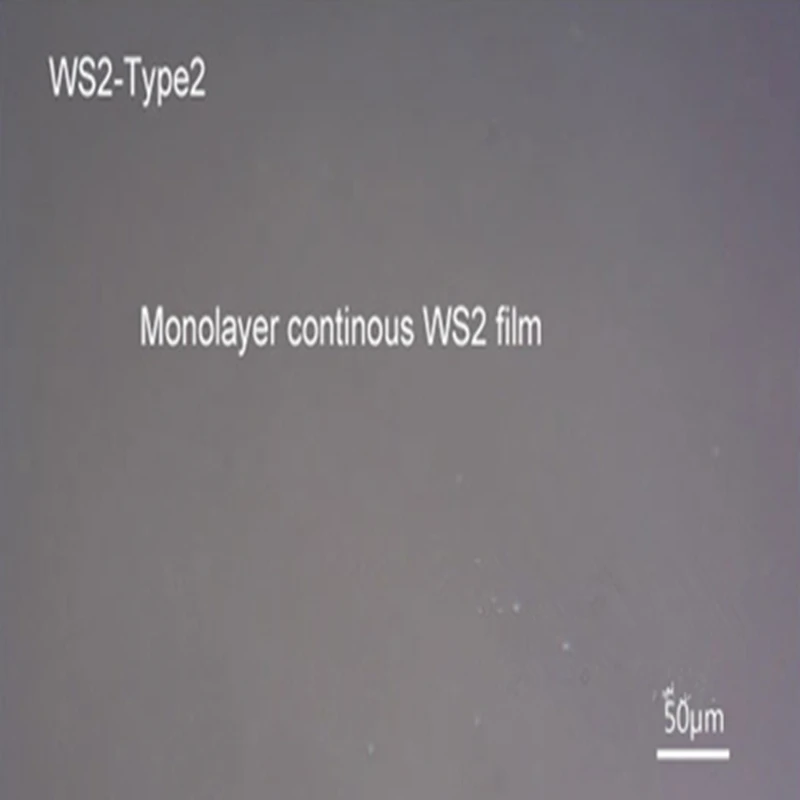
Sapphire substrate WS2                                                        Single layer WS2 isolated die ABUIABACGAAgxvKt3AUonb_KLjDUAjicAg_  WS2-flakes_

                                                                                         Single layer WS2 continuous film

WS2-type1__  WS2-type2_

Single double layer hybrid WS2

WS2-flakes-mono-bilayer_  WS2-type3_

Sapphire base single layer WS2 (4 inches)

web-4inch-monoalyer-WS2_  ABUIhffKBxACGAAg8u7m0gUo8K3osQQw9AM4iQM!400x400_

__


Смотрите так же другие товары: