

Новое поступление

2/4/6 шт. оригинальная капсула VOOPOO V.THRU Pro 0 3 Ом/1 2 Ом мл |
823,81 - 1 740,15 руб.

Ethernet W5100 Плата расширения сети модуль SD карта мега | Электроника
913,64 руб.

Плата расширения сети Ethernet W5100 R3 поддерживает MEGA | Электроника
1 896,46 руб. / набор

Плата расширения Raspberry pie CM4 плата нагрузок/raspberry PI ShuangQian Мега Ethernet порты R2S/R4S
2 515,44 - 15 272,32 руб.

Полноцветный светодиодный видеоэкран HUIDU R501S приемная карта обновленная модель
2 500,17 руб.

Бесплатная доставка 10 шт. AO4407A AO4408 AO4409 AO4410 AO4411 AO4412 AO4413 AO4414 новый оригинальный

SUPTEC Cable Organizer Wire Silicone Winder Charger Management Clips Holder Protector for Mouse Earphone Headphone | Электроника
151,82 - 340,48 руб.

MBM-Chip Store
Магазина MBM-Chip Store работает с 06.05.2014. его рейтинг составлет 93.87 баллов из 100. В избранное добавили 1443 покупателя. Средний рейтинг торваров продавца 4.8 в продаже представленно 3588 наименований товаров, успешно доставлено 2204 заказов. 864 покупателей оставили отзывы о продавце.
Характеристики
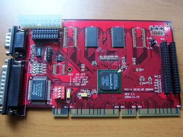
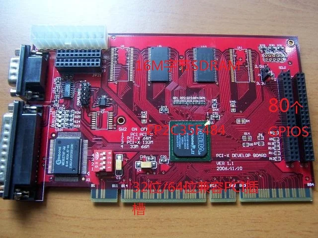
S1800 PCI development board 32/64 bit FPGA platform winder | Электроника
История изменения цены
*Текущая стоимость 24 680,08 уже могла изменится. Что бы узнать актуальную цену и проверить наличие товара, нажмите "Добавить в корзину"
| Месяц | Минимальная цена | Макс. стоимость | Цена |
|---|---|---|---|
| Sep-17-2025 | 29369.45 руб. | 30837.37 руб. | 30103 руб. |
| Aug-17-2025 | 29122.33 руб. | 30578.9 руб. | 29850 руб. |
| Jul-17-2025 | 24433.86 руб. | 25655.1 руб. | 25044 руб. |
| Jun-17-2025 | 28629.21 руб. | 30060.81 руб. | 29344.5 руб. |
| May-17-2025 | 24927.41 руб. | 26173.34 руб. | 25550 руб. |
| Apr-17-2025 | 28135.66 руб. | 29542.82 руб. | 28838.5 руб. |
| Mar-17-2025 | 27888.93 руб. | 29282.27 руб. | 28585 руб. |
| Feb-17-2025 | 27642.17 руб. | 29024.30 руб. | 28333 руб. |
| Jan-17-2025 | 27395.13 руб. | 28765.26 руб. | 28080 руб. |
Описание товара


S1800PCI-X FPGA development experimental board using 32/64 bit PCI / PCI-X interface, user-friendly self-development, the user can design their own application patch panels,
Such as external A / D data acquisition, image data processing and other system applications, without the need for PCI / PCI-X interface has too much understanding. The core FPGA chip uses ALTERA company
Of the new CYCLONE2 FPGA series, EP2C35F484C8, the capacity of 35,000 logic macrocell, equivalent to the standard 1 million logic gate, the speed of -8,
Compiled system speed can reach 100MHz, can support ALTERA's SOPC core NIOS2 system development, NIOS2 development environment can be compiled after the
The implementation of the file can be downloaded through the PCI interface to the development board FLASH to the maximum 100 users available IO;
Development board function description:
PCI interface external bus interface supports 8,16,32,64-bit data bus, and CPU, SDRAM, FIFO, external interface chip and other equipment directly connected.
The following is the FPGA development board internal IP core interface:
PCI bus 2.3 standard, 32/64 bit bus, 33/66M support, fully VHDL source code designed to provide;
PCI-X bus 2.0A standard, 64-bit bus, 66M / 100M support, fully VHDL source code designed to provide;
Support PCI / PCI-X bus configuration read, configure write;
Support PCI / PCI-X bus IO read, IO write;
Support PCI / PCI-X bus BUS MASTER read, BUS MASTER write;
Support PCI-X split transmission protocol, increase bus efficiency;
Support internal DMA interrupt and external bus input interrupt generation;
Support a PCI IO space, the size of 256 bytes;
Support a PCI memory space, the size of 4M bytes;
Support PCI burst access, burst length of 8 to 128 double word length;
Users can define their own device ID and manufacturer ID;
1 FPGA internal 16C950 serial port, fully VHDL kernel provided;
1 group 4MX64 bit SDRAM, the maximum capacity to support 64MX64 bit SDRAM interface, 133M maximum operating frequency, fully VHDL kernel SDRAM interface source code;
4 LED status indicator outputs that provide debugging and test use, fully available in VHDL kernel source code;
External interface 5V / 3.3V / 2.5V / 1.8V interface support, support LVDS interface input and output;
External expansion standard 32/64 bit data bus, providing dma data transfer capability, up to 80 users can use the IO, to provide LVDS input and output functions;
The above functions are provided with PCI interface for access and operation, providing DOS, WINDOWS98 / WINDOWS2000 / XP driver and test program source code.
Applications:
Data acquisition, a / d, d / a data transformation, data processing
Pci data buffering, data encryption;
industrial control;
Performance and compatibility, stability testing
The PCI development board is tested on the following PC and is powered on normally:
Performance test using the maximum cycle of transmission, each DMA block size of 512K bytes, according to the average 5 seconds flow calculation, by the number of seconds to transfer the number of DMA block calculation.
32 bit / 33M PCI:
CPU Memory Motherboard Chipset Operating System DMA Read DMA Write
P4 2.4G 256M DDR 915P 800 FSB WIN2000 93M bytes / sec 112M bytes / second
64 bit / 66M PCI:
CPU Memory Motherboard Chipset Operating System DMA Read DMA Write
XEON 2.8G 512M DDR E7205 WINXP 425M bytes / sec 463M bytes / second
64-bit / 66M PCI-X
CPU Memory Motherboard Chipset Operating System DMA Read DMA Write
XEON 2.8G 512M DDR E7205 WINXP 402M bytes / sec 438M bytes / sec
64 bit / 100M PCI-X
CPU Memory Motherboard Chipset Operating System DMA Read DMA Write
XEON 2.8G 512M DDR E7205 WINXP 611M bytes / sec 671M bytes / second
Free ALTERA QUARTUS2 6.0 development tools CD;
Free NTDDK and DRIVERWORKS driver development tools CD;
Development board support AS and JTAG download, with the development board free ALTERA
BYTEBLASTER 2 download a cable for users to use;
Http://www.mbm-chip.com
Смотрите так же другие товары: